- Capacitors
The Road to Thinner MLCCs and New Product Development
Introducing the material process for thinning the layers of highly reliable MLCCs and the road to new product development.
Overview
As electronic devices become smaller and more sophisticated, multilayer ceramic chip capacitors (MLCCs) are becoming smaller and thinner, and there is a need to develop highly reliable MLCCs that can operate even under harsh conditions. However, there are challenges in making the layers thinner, and various technological advances have been required.
Special Feature Page
Material Process Issues for Thinner Layers
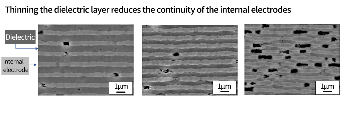
With conventional technology, there was a problem that making the dielectric layer thinner reduced the continuity of the internal electrodes.
As the layers were thinner, unevenness in the internal electrodes, coarse particles in the dielectric layer, impurities, and defects became larger and larger defects, leading to an increase in short circuits, a decrease in voltage resistance, and reduced reliability. It was also assumed that thinning the layers would reduce the number of particles per layer, which would lead to reduced reliability.*1。
*1: For details on how the number of particles per layer contributes to high reliability, please see Evaluation and Analysis Technology Visualizes Areas of Deterioration
Therefore, it became important to develop new material processes for thinning the layers.
Evolution of Thin Layer Technology
To achieve even thinner layers, it was necessary to evolve each of the elemental technologies for dielectrics, internal electrodes, and firing, as well as to evolve the technology to combine these new elemental technologies.
We will introduce our work on internal electrodes as an example of thin-layer technology.
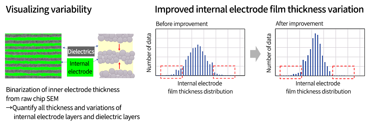
The raw chip SEM was binarized to quantify the thickness and variation of the internal electrode layer and dielectric layer. The variation of the internal electrode film thickness was improved by reducing the diameter of the Ni particles and improving the particle size distribution, co-material size, plate cylinder design, and paste rheology (red frame in the graph).
Thus, designing for variation/local defects is particularly important in thin layer technology.
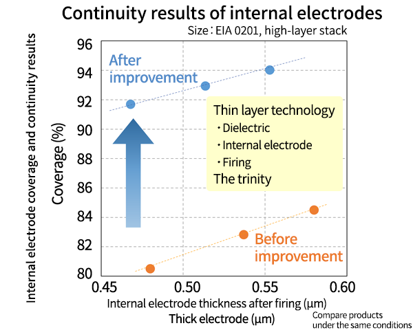
Continuity results of internal electrodes using thin layer technology
By combining improvements to the internal electrodes with thin-layer technology for dielectrics and firing, we were able to achieve an improvement of approximately 10% and coverage from the 80% range to the 90% range at the same thickness ratio (EIA 0201 size, high-layer stack).
Furthermore, as shown in the left figure, even with an internal electrode thickness of 0.45 μm, good continuity of over 90% coverage was maintained, and we were able to achieve a thin dielectric layer and high coverage and thin internal electrode layer.
However, since the internal electrode is still thicker than the dielectric, it is believed that the internal electrode can be made even thinner. We will continue to work on developing even thinner layer technology.
New Product Development and World-Leading Announcements
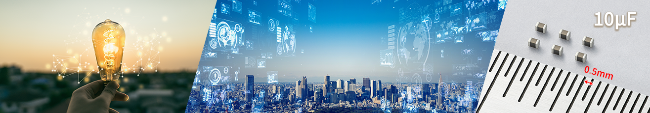
The development of the material process, evaluation and analysis technologies led to the release of an EIA 0201 size product with a capacitance value of 10 μF, the highest capacitance class in the industry*2 and a world-leading announcement.
*2: Among MLCCs in the 0201 case size (KYOCERA research, March 2023)
Temperature Characteristics | X5R (EIA) |
|---|---|
Operating Temperature Range | -55℃ to +85℃ |
Temperature Coefficient | ±15% |
Capacitance | 10μF |
Capacitance Tolerance | K(±10%)、M(±20%) |
Dissipation Factor | 10% MAX. |
IR | 50MΩ・μF MIN. |
Rated Voltage | 4.0Vdc |
Data is based on research by Kyocera.
Special Feature Page
EIA 0201 Size MLCCs with the Industry's Highest*2 Capacitance of 10μF
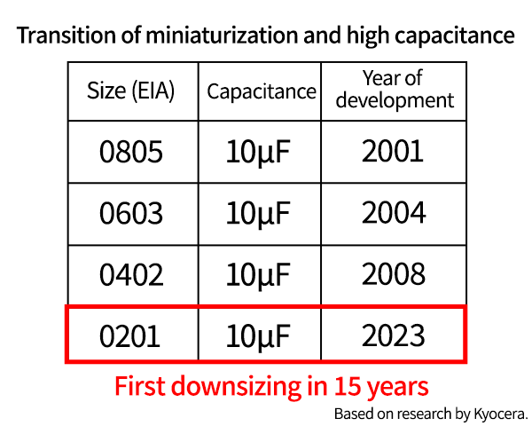
MLCC size trends
In terms of the development of MLCCs worldwide, EIA 0805 10μF was developed in 2001, EIA 0603 10μF in 2004, and then EIA 0402 10μF in 2008, four years later (according to Kyocera). And the EIA 0201 10μF developed by Kyocera in 2023 was the first downsizing in 15 years.
Kyocera will continue to develop MLCCs in line with market trends toward smaller size and higher capacity.
Kyocera will continue to pursue industry-leading MLCC development
that contributes to the advancement of society and humankind

Related Links
Capacitors Catalog (PDF/1.4MB)
Click Here for Find All MLCC Products
The Important Information/Disclaimer is incorporated in the catalog and/or this page by reference and should be reviewed in full before placing any order or inquiry.
Related Keywords
Technical information View All


 Contact & Support


Search by part number
Search by keyword
Search by category
-
- SAW Devices
- Advanced KYOCERA AVX Components
Search by Applications
Distributor Inventory Search
Please enter the model name of Kyocera. You can search up to 3 types at the same time.