- Crystal Devices
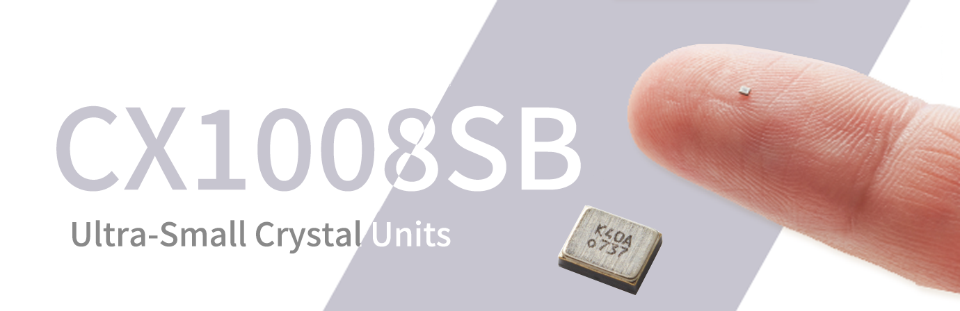
Ultra-Small Crystal Units CX1008SB Series

The increasing functionality of communication terminals has led to an increase in the mounting density of electronic devices and a reduction in the mounting area, leading to demand for smaller mounting components.
In this market context, Kyocera has developed our new ultra-small crystal unit CX1008SB Series available for mass production.
Overview
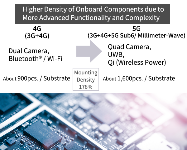
In recent years, the mounting density of electronic devices has increased due to the increasing number of functions of communication terminals for 5G communications, faster Wi-Fi, and the electrification of onboard components. In addition, due to the limited space available in the mounting area, the size of mounted components is becoming smaller.
Among them, Kyocera developed excellent photolithography and ultra-high precision machining technology jointly with Osaka University (Plasma CVM technology), and we have succeeded in mass-producing an ultra-small crystal unit, the CX1008SB Series.
Bluetooth® is a registered trademark of Bluetooth SIG, Inc.
Challenges and Solutions in Miniaturization
If the size is reduced from the conventional size of 1.2 x 1.0mm to 1.0 x 0.8mm, the series resistance value (CI value) will increase by about 30%. To avoid this, it was necessary to review the circuit design of the substrate on which the crystal mounts.
Therefore, by optimizing the design of the crystal device using Kyocera's proprietary piezoelectric analysis technology, Kyocera achieved a size as small as 1.0 x 0.8mm while also achieving electrical characteristics equivalent to 1.2 x 1.0 mm*1. This made it possible to use the circuit on the board without making changes.
*1 Kyocera's product CX1210 Series
Data is based on research by Kyocera.
Features
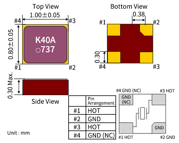
| Size (mm) | L x W=1.0 x 0.8 T=0.30 Max. |
|---|---|
| Frequency Range (MHz) | In Mass Production 37.4, 40, 59.97 Under Development 38.4, 48, 76.8 |
| Initial Frequency Deviation | +/- 10ppm (@+25℃) |
| Frequency Temperature Characteristics | +/- 12ppm (-30 to +85℃) |
Series Resistance
| 37.4 MHz | 38.4 MHz | 40 MHz | 48 MHz | 59.97 MHz | 76.8 MHz |
|---|---|---|---|---|---|
| 60Ω Max. | 60Ω Max. | 60Ω Max. | 60Ω Max. | 50Ω Max. | 35Ω Max. |
CX1008SB Series Product Search Catalog (709KB)
Applications

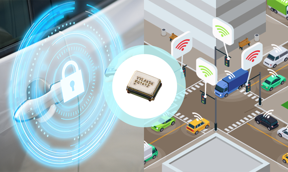
GNSS, 5G millimeter-wave compatible smartphones, Wi-Fi® module, etc.

Manufacturing Technology for Small, High-Precision Quartz Devices
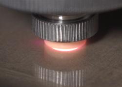
Plasma CVM Machining
With conventional machining accuracy, when a crystal device is miniaturized, there is a problem that variations in electrical characteristics become large.
Kyocera has solved this problem with its ultra-high precision machining technology (plasma CVM technology), which Kyocera developed in collaboration with Osaka University.
This technology is a processing method that uses neutral radicals in plasma and chemical reactions on the surface of the workpiece, enabling precise control of crystal thickness and surface conditions. This has resulted in a successful reduction in frequency variability.
Keywords The Official Mascot of Kyocera’s Electronic Components: Eletan
Click here to learn more about Eletan
What is CVM?
It stands for Chemical Vaporization Machining.
Kyocera is developing a variety of products based on these technologies, including low-frequency oscillators for use in vehicles and high-frequency oscillators and high-precision oscillators for base stations.
Through the development of new products, we will support a society in which IoT is advancing, including fifth-generation mobile communication systems and advanced driver assistance systems (ADAS), which are expected to be further developed in the future.
Related Links
Related Keywords
Technical information View All

 Contact & Support


Search by part number
Search by keyword
Search by category
-
- SAW Devices
- Advanced KYOCERA AVX Components
Search by Applications
Distributor Inventory Search
Please enter the model name of Kyocera. You can search up to 3 types at the same time.