Design specifications of printed wiring board
Since the amount of solder (fillet size) for mounting a capacitor on a printed circuit board influences the capacitor directly, sufficient consideration is necessary. Confirm the suitable land pattern size in order to decide the suitable amount of solder.
When the amount of solder is too much, stress on a capacitor increases. It may cause a crack in the
capacitor. When a land design of a printed wiring board is considered, it is necessary to set up the form
and size of the land pattern so that the amount of solder is suitable.
When the amount of solder is too little, the adhesion (shear) strength of the terminal electrode may be
insufficient, and the capacitor may drop off from the printed wiring board. The reliability of the circuit
may also be affected.
Recommendation for land pattern size to which the amount of solder does not excessively increase.
![[Recommended land pattern size of each case size]](/sites/default/files/assets/static/mlcc-handling_mounting_contents01_01.png)
(Unit: mm)
|
Size
|
Code
|
Dimension
|
Recommended land pattern dimensions
|
||||
|---|---|---|---|---|---|---|---|
|
JIS
|
EIA
|
L
|
W / T
|
a
|
b
|
c
|
|
|
02
|
0402 | 01005 | 0.4 ± 0.02 | 0.2 ± 0.02 | 0.13 ~ 0.20 | 0.12 ~ 0.18 | 0.20 ~ 0.23 |
|
03
|
0603 | 0201 | 0.6 ± 0.03 | 0.3 ± 0.03 | 0.20 ~ 0.25 | 0.25 ~ 0.35 | 0.30 ~ 0.40 |
| 0.6 ± 0.05 | 0.3 ± 0.05 | ||||||
| 0.6 ± 0.09 | 0.3 ± 0.09 | 0.23 ~ 0.30 | 0.25 ~ 0.35 | 0.30 ~ 0.45 | |||
|
05
|
1005 | 0402 | 1.0 ± 0.05 | 0.5 ± 0.05 | 0.30 ~ 0.50 | 0.35 ~ 0.45 | 0.40 ~ 0.60 |
| 1.0 ± 0.15 | 0.5 ± 0.15 | 0.40 ~ 0.60 | 0.40 ~ 0.50 | 0.50 ~ 0.75 | |||
| 1.0 ± 0.20 | 0.5 ± 0.20 | ||||||
|
105
|
1608 | 0603 | 1.6 ± 0.10 | 0.8 ± 0.10 | 0.70 ~ 1.00 | 0.80 ~ 1.00 | 0.60 ~ 0.90 |
| 1.6 ± 0.15 | 0.8 ± 0.15 | 0.80 ~ 1.00 | 0.80 ~ 1.00 | 0.80 ~ 1.10 | |||
| 1.6 ± 0.20 | 0.8 ± 0.20 | ||||||
| 1.6 ± 0.25 | 0.8 ± 0.25 | ||||||
|
21
|
2012 | 0805 | 2.0 ± 0.10 | 1.25 ± 0.10 | 1.00 ~ 1.30 | 1.00 ~ 1.20 | 1.00~ 1.45 |
| 2.0 ± 0.15 | 1.25 ± 0.15 | 1.00 ~ 1.30 | 1.00 ~ 1.20 | 1.25~ 1.55 | |||
| 2.0 ± 0.20 | 1.25 ± 0.20 | ||||||
|
316
|
3216 | 1206 | 3.2 ± 0.20 | 1.6 ± 0.15 | 2.10 ~ 2.50 | 1.10 ~ 1.30 | 1.40 ~ 1.90 |
| 3.2 ± 0.20 | 1.6 ± 0.20 | 2.10 ~ 2.50 | 1.10 ~ 1.30 | 1.60 ~ 2.00 | |||
| 3.2 ± 0.30 | 1.6 ± 0.30 | ||||||
|
32
|
3225 | 1210 | 3.2 ± 0.30 | 2.5 ± 0.20 | 2.10 ~ 2.50 | 1.10 ~ 1.30 | 1.90 ~ 2.80 |
NOTE(1)The creepage distance of basic insulation may be required to be 2.5 mm or more. (See JIS C 6950-1) Therefore, the dimension of "a" for safety standard certified capacitors is recommended to be 3.0 mm to 3.5 mm. When using a safety standard certified capacitor, consider a slit between lands or cleaning, etc. to prevent electrical discharge from creepage.
When mounting two or more capacitors are mounted on the common land, it is necessary to separate the land
with the solder resist strike so that it may become the exclusive land of each capacitor.
Unrecommended and recommended examples shown as following.
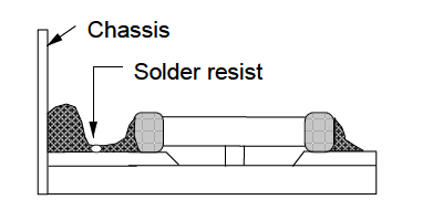
Recommended and unrecommended examples of soldering
|
Mounting
characteristic |
Unrecommended
|
Recommended
|
|---|---|---|
|
Mounting with
leaded component |
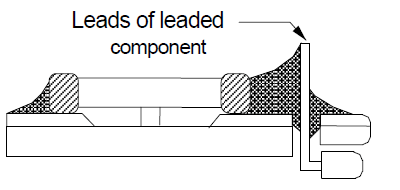 |
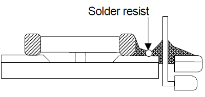 |
|
Mounting on the
vicinity of chassis |
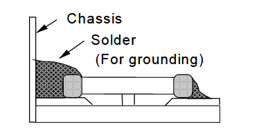 |
 |
|
Wire soldering
after mounting |
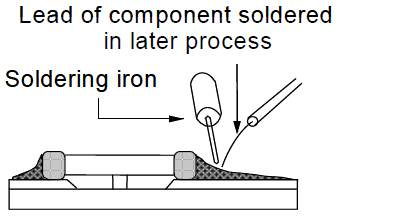 |
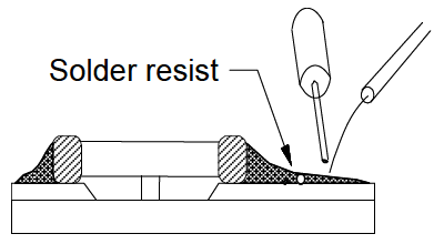 |
|
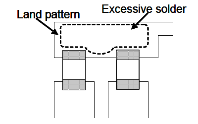
Common solder land with other chip capacitors(2)
|
 |
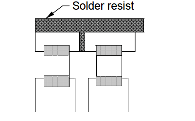 |
NOTE(2) When a capacitor is mounted on a common solder land with another SMD, design the solder resist pattern so that the effective land pattern for the capacitor is exclusive and does not have excess solder.
Safety Application Guide for Multilayer Ceramic Chip Capacitors All Lists
 Contact & Support


Search by part number
Search by keyword
Search by category
-
- SAW Devices
- Advanced KYOCERA AVX Components
Search by Applications
Distributor Inventory Search
Please enter the model name of Kyocera. You can search up to 3 types at the same time.