Placement of the capacitor to printed wiring board
After soldering a capacitor on a printed wiring board, if it is bent during board cutting, board
cropping,board checking, component mounting, mounting to a steel case, flow soldering of the back of the
board after reflow soldering, or handling, a crack may occur in the capacitor.
Confirm the mounting position and direction that minimizes the stress imposed on the capacitor during
flexing or bending the printed wiring board.
Recommended mounting arrangement and direction that minimizes the stress imposed on the capacitor during
flexing or bending of the printed circuit board is shown as following.
| Condition | Unrecommended | Recommended |
|---|---|---|
| Bending or flexing | 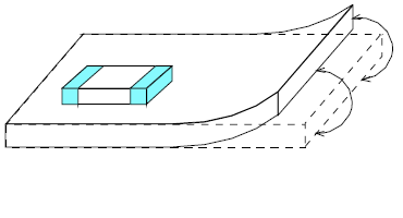 |
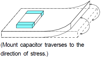 |
Since mechanical stress depends on the position and direction in which the capacitor is mounted near the cutting line, please refer to the following figure.

When dividing the printed wiring boards, the intensities of mechanical stress applied to capacitors are
different by each dividing method is in the order of: Push-back < Slit < V-groove < Perforation.
Therefore, consider not only position of capacitors, but also way of dividing the printed wiring board.
Separation of multiple printed circuit board
A multiple printed circuit board is divided into each unit board after soldering. If excessive bending
stress is applied to the board, a crack may occur in the capacitor. Carry out sufficient consideration for
stress control at the time of cutting with reference to the following figures.
Bending stress and recommended placement of capacitor when printed circuit board is cut.
| Point | Unrecommended | Recommended |
|---|---|---|
| Direction
of bending |
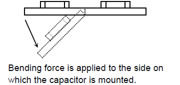 |
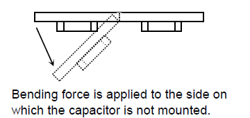 |
| Orientation of
capacitor |
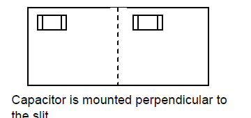 |
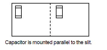 |
| Distance from
a slit |
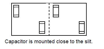 |
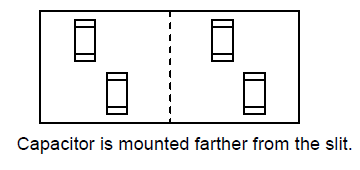 |
Safety Application Guide for Multilayer Ceramic Chip Capacitors All Lists


